ic programmer|chip test|automated programmer system|Automated Device Programmers

Microelectronics
Provide chip testing and programming services

2026-04-01

2026-03-31

2026-03-24

2026-03-23

2026-03-20

2026-03-19
Address:3rd Floor, No. 4 Factory Building, No. 550, Jujin Road, Zhangpu Town, Kunshan City
Phone:0512-57225603
Mobile:13812682041Miss Zhao
Email:jessie@ptchip.com.cn
author::Microelectronicsrelease date:2020-11-21Viewers:4671
Shenzhen Angke Technology Co., Ltd., a professional IC burner manufacturer, has launched a dedicated engineering and mass production burner for Universal Flash Storage (UFS), as well as automated burning equipment. The newly launched new generation burner integrates the design and application of the UFS system, and is suitable for R&D, product verification, and factory small batch and mass production requirements.
In January 2018, UFS 3.0 was officially released. As an iterative upgrade product of UFS 2.0 and 2.1, UFS 3.0 has brought very significant improvements and advancements in performance. However, this flash memory is not officially commercially available, so we have no way of knowing its actual performance.
A few days ago, a screenshot of Androbench reading and writing test records of 1TB UFS 3.0 flash memory was exposed on the Internet.
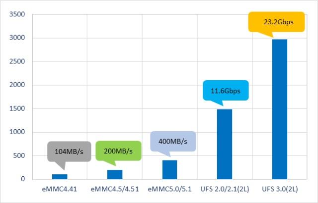
From this record, we can clearly see that the sequential read speed of UFS 3.0 reached 2279.8MB/s, and the sequential write speed reached 1801.1MB/s. According to the current 700-800MB/s sequential reading speed of UFS 2.1, it is basically 2-3 times.

However, UFS 3.0's 4K read-on-read and write-on-write results are not much different from the existing UFS 2.1, and there is still room for optimization.
According to the previous introduction, UFS (Universal Flash Storage) 3.0 focuses on high performance and low power consumption. It is the first flash memory to introduce the MIPI M-PHY HS-Gear4 standard, with a single channel bandwidth up to 23.2Gbps, which is UFS 2.0/2.1 Twice.

In addition, UFS 3.0 supports more partitions, upgrades the ability to correct errors, the voltage reaches 2.5V, and supports the latest NANG Flash media.
The mainstream flagship chips in 2019 all support UFS 3.0, and it has been determined that Qualcomm Snapdragon 855 and Samsung Exynos 9820 are compatible with this new flash memory specification. Samsung has also stated that it expects to launch models with UFS 3.0 flash memory in the first half of this year. It is currently speculated that the Samsung Galaxy S10 series should have a product that uses UFS 3.0 flash memory, which may be the top-equipped S10+ 5G version.

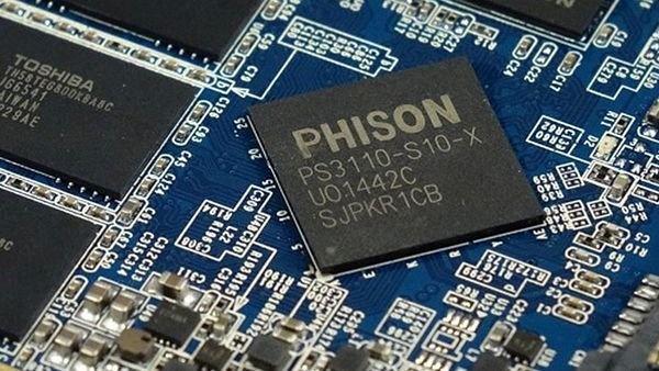
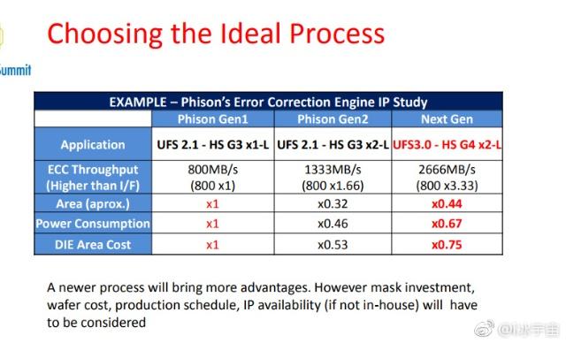
Previously, Taiwanese manufacturer Phison had announced the development process on UFS flash memory. Phison's UFS 2.1 is divided into two generations of products, with throughputs of 800MB/s and 1333MB/s, and the latest UFS 3.0 has a throughput of 2666MB/s, which is basically doubled compared to UFS 2.1.

It seems that it may take some time for UFS 3.0 products to be launched, but its actual performance should greatly exceed the existing UFS 2.1 products. We might as well look forward to it.
Hot tags: