ic programmer|chip test|automated programmer system|Automated Device Programmers

Microelectronics
Provide chip testing and programming services

2026-03-23

2026-03-20

2026-03-19

2026-03-18

2026-03-17

2026-03-16
Address:3rd Floor, No. 4 Factory Building, No. 550, Jujin Road, Zhangpu Town, Kunshan City
Phone:0512-57225603
Mobile:13812682041Miss Zhao
Email:jessie@ptchip.com.cn
author::Microelectronicsrelease date:2020-11-21Viewers:3437
Analyze the programming structure of NAND Flash
In the previous article, we introduced the difference between NAND Flash and NOR Flash. From the perspective of structure and principle, the ROM-like structure of NOR Flash makes it easy to program. Therefore, many engineers are used. If the cost is not too high, NAND Flash simply cannot survive.
NAND Flash is more and more popular with consumers due to its low price and large storage capacity, especially consumers who need to store large amounts of data. What should be paid attention to when programming NAND Flash?
Partition
The essence of defining a partition is to define how data will be written to NAND Flash, and data of different contents is written to the corresponding address. General users will have multiple areas, such as boot, kernel, fs, user and other partitions.
Partition description: partition address range (start block, end block), image file size (Image Size).
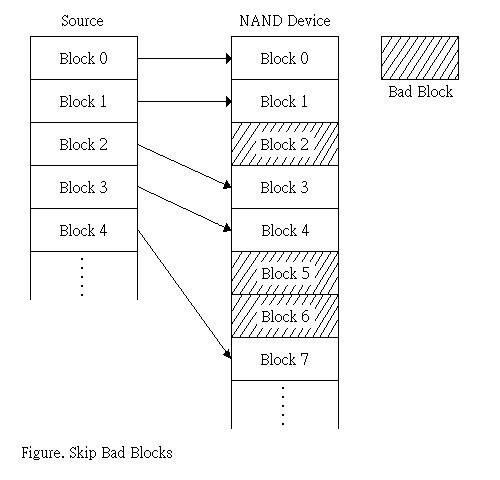
Partition data storage: the mirror file is stored from the starting block of the partition. If there are bad blocks in the partition, the bad block processing strategy will be used to replace the bad blocks until the end of the mirror file. If the partition is not good enough to store the mirror file, then Burning failed.
The following figure is a schematic diagram of the image file partition burning with skipped bad blocks:

ECC in the spare area (OOB)
ECC exists in the Spare Area of each page of NAND. It allows the external system to find out whether the data in the main area is incorrect. In most cases, the ECC algorithm can correct errors, and bad blocks may also occur in NandFlash in use, so ECC is very necessary.
Different users may use different ECC algorithms. Generally speaking, the ECC algorithm is provided by the processor supplier. If the ECC algorithm is not included in the programmer software, the user needs to provide the ECC algorithm source code.
If the user does not use the imported file, but uses the method of reading the master, and there is no dynamic data, the ECC algorithm can be ignored, because the spare area in the master has already calculated the ECC, and the spare area of the master is directly changed Just copy to other chips.
Bad Block Management (Bad Block Management)
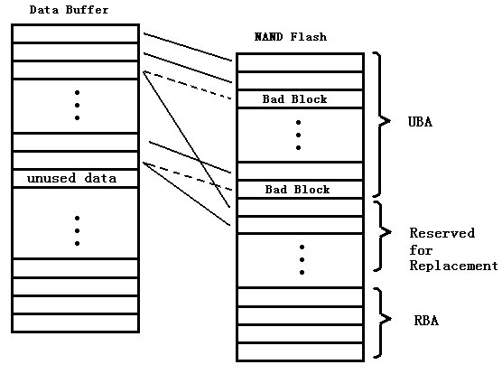
The bad block handling strategy defines how the algorithm should deal with bad blocks. The basic bad block handling strategies include skipping bad blocks, replacing tables (Reserve Block Area, RBA), and so on.
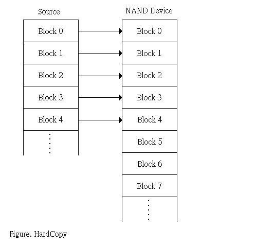
● Hard copy
In fact, hard copy means nothing is dealt with when encountering bad blocks, no matter the good block or the bad block is burned directly, even if the verification data is inconsistent, no error will be reported;

● Skip bad blocks
To skip the bad block is to jump to the next good block to burn when encountering a bad block;

就是预留一些块作为保留块,是用于替换坏块用,当遇到坏块时,在保留区中选一个块来替换,将原来写到坏块的数据写到替换块中。

● BBT (Bad block table)
In fact, it is to skip bad blocks, and then write a bad block table (Bad block table) in the designated location of the Nand flash memory. The figure below is the structure diagram of BBT.

Transfer from: Zhiyuan Electronics
Previous:Analysis of Nand Flash Storage Structure
Next: 没有了!
Hot tags: